

Author animation, 24 Aug 2026. Copper loss versus an optical pulse — illustration only. Not a measurement, and not a reprint of the Nature figures.
This weekend in Washington, DC, I read the full Nature Electronics review on co-packaged optics — not the abstract. Kim et al., published 19 August 2026. The next day, SK hynix put up a newsroom piece that uses the same numbers and a different sentence.
The paper is a domain review. It does not say what SK will ship.
The newsroom is a translation: chips → systems, HBM → the rack, optics → the memory interface.
A six-chart walkthrough of the packaging argument:


Those charts, and the ones below, are reconstructions. They are not reprints of the Nature figures. SK’s official adapted diagrams live in the newsroom post.
1. Two documents, one weekend
The review does what a good review should do. It puts HPC/AI in a communication-limited regime. It walks the packaging ladder from 2D side-by-side to 2.5D interposers to 3D hybrid bonding to monolithic integration. It tables components and commercial platforms. It lists the unglamorous constraints: lasers, thermal drift, coupling, yield, the missing picojoules in SerDes and DSP.
Seunghoon Hong of SK hynix AI Infra is a corresponding author. That is affiliation and framing, not a product SKU.
The newsroom (20 August) keeps the metrics and changes the customer. HBM already fixed the bottleneck inside the accelerator package. Hyperscale clusters now stall on data movement between systems. CPO is framed as the way to extend HBM innovation to the system, not as a replacement for HBM. The long draw is optical connectivity to the memory interface — an XPU pool talking to a memory pool over a photonic interposer.
Kyusang Lee (UVA):
Even if computing chips become more powerful, overall system performance cannot improve unless data movement between chips keeps pace.
Seunghoon Hong (SK Hynix):
CPO integrates optical transceivers into the same package as the processor… This fundamentally changes how data moves through AI systems.
The review inventories a field. The newsroom tells you why a memory vendor signed the inventory.
SK newsroom: https://news.skhynix.com/en/cpo-in-nature-electronics/
SK X (official adapted figures):


2. The bandwidth wall — four rates, not three
The review’s scaling discussion is the only chart that matters, and it is easy to misread.
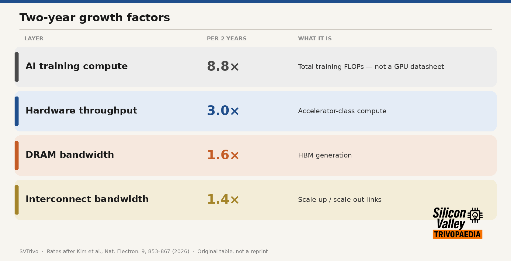
HBM is the layer that partially caught up inside the package. The rack did not. If you flatten 8.8× into “hardware is exploding,” the rest of the paper becomes a transceiver brochure.
SK’s official adapted chart drops the DRAM line and keeps three curves: models 8.8×, hardware 3.0×, interconnect 1.4×. Cleaner for a press post. Worse for the HBM argument. The 1.6× line is why “just stack more HBM” is not an interconnect strategy.
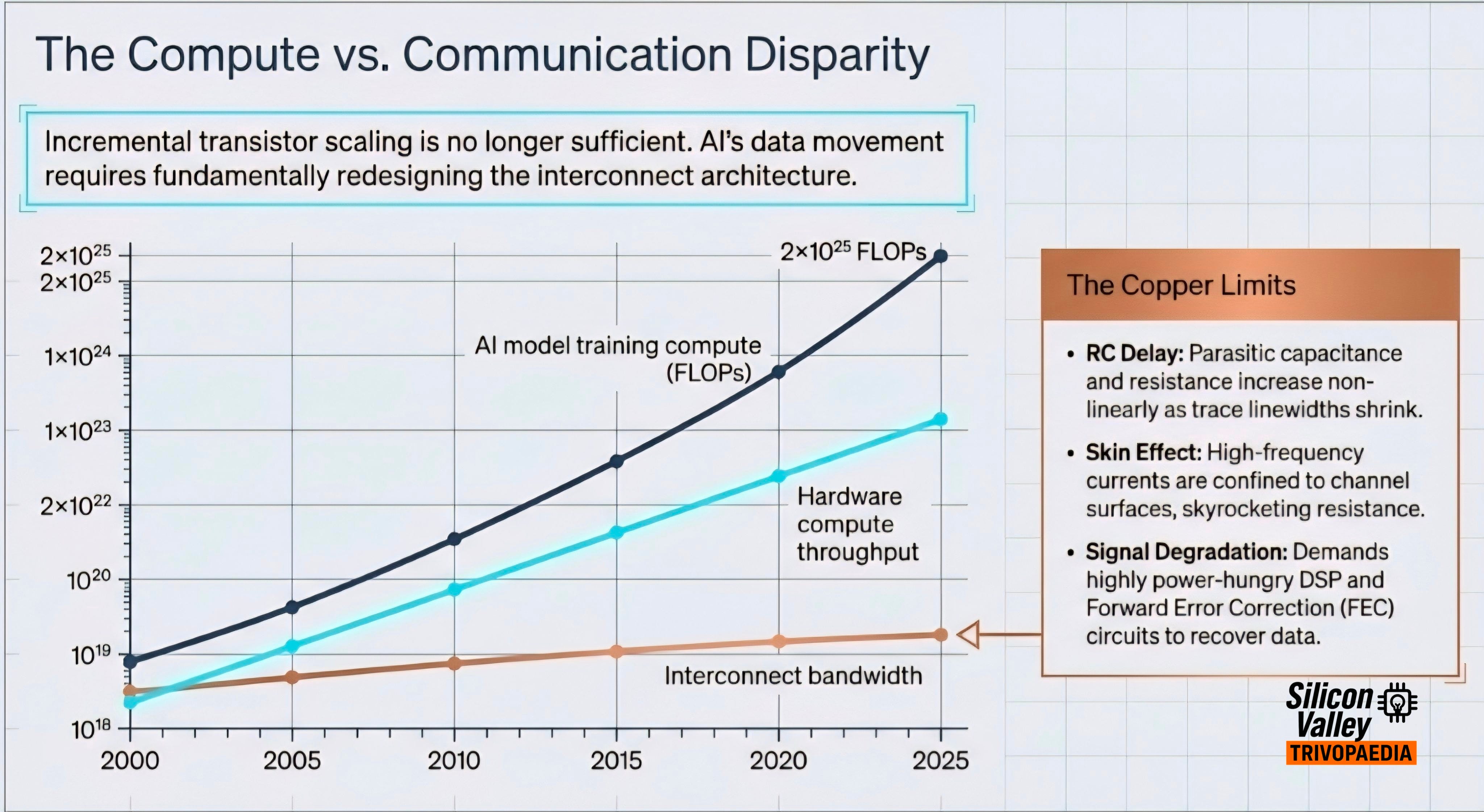
Copper’s side of the wall is not mysterious. RC delay, skin effect, and the DSP/FEC latency and power required to recover a rotten electrical eye. That is why “the optical modulator is 0.1 pJ/bit” never equals “the link is 0.1 pJ/bit.”
3. Three numbers that have to land together
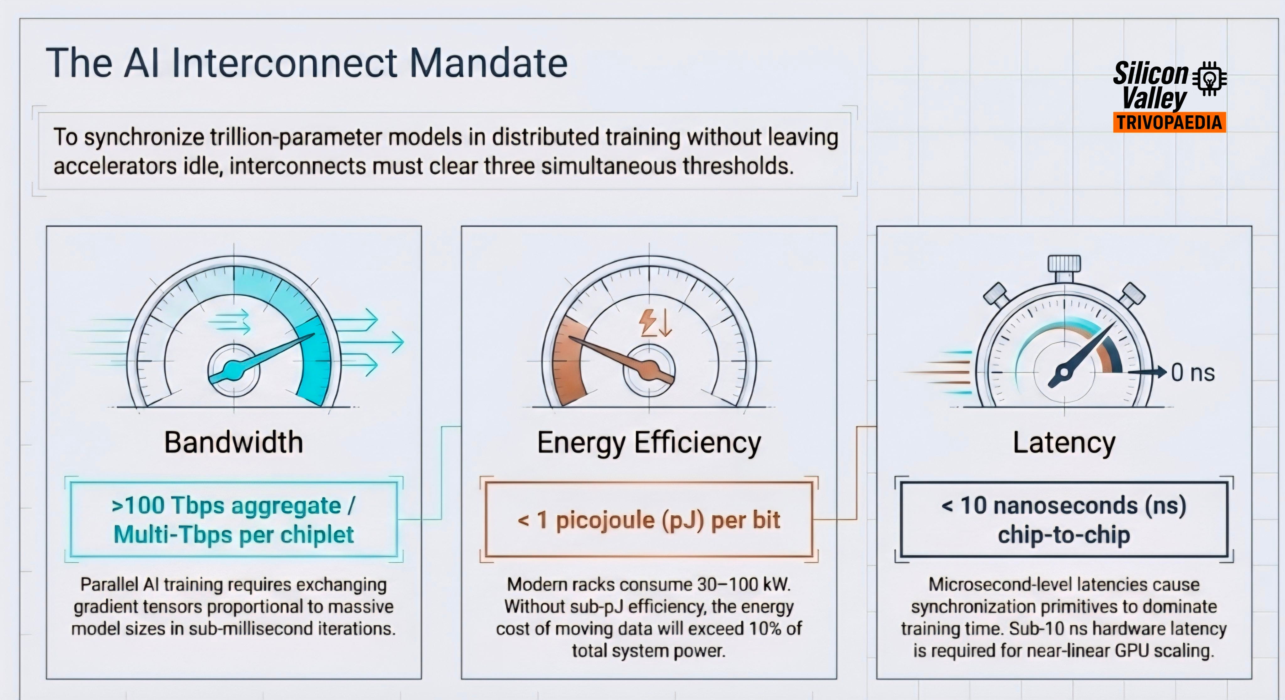
The review’s system target, repeated in the newsroom:
Bandwidth: >100 Tbps class per node
Energy: <1 pJ/bit
Latency: <10 ns chip-to-chip
Miss any one of them and AllReduce turns GPUs into expensive heaters.
Lee lists four reasons CPO can become infrastructure rather than a cable: bandwidth density, energy-distance, parallel fan-out, immunity to EMI. Fair. None of those four is a 2026 GPU-package shipping spec.
4. The roadmap is packaging
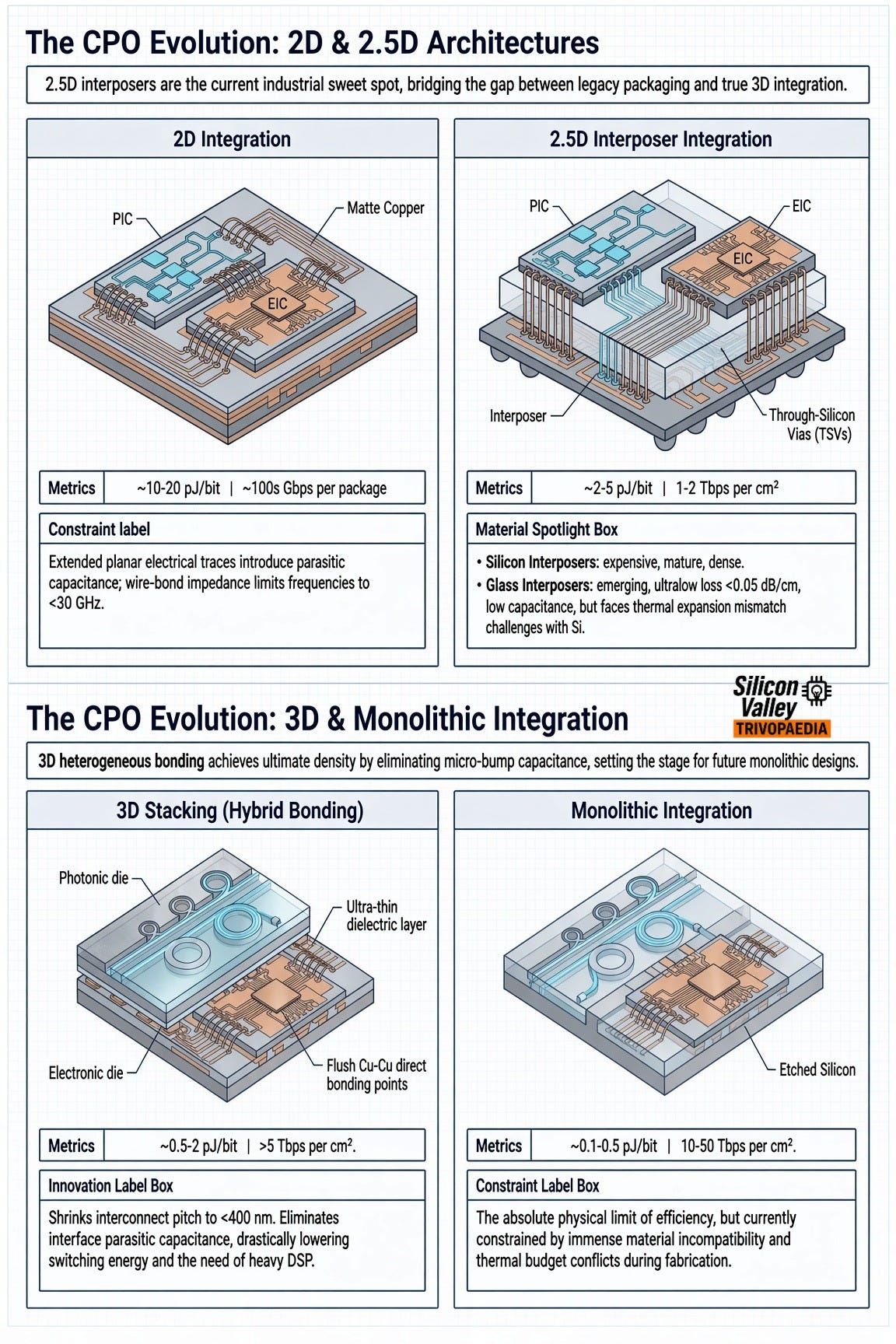
2D: PIC and EIC side by side. Cheap. Long electrical hop.
2.5D: where the industry actually is — silicon or glass interposer.
3D hybrid bonding: Cu–Cu, bump capacitance gone.
Monolithic: best on a slide, meanest in a fab.
The platforms the review names — Broadcom-class fabrics, NVIDIA Spectrum-X / Quantum-X photonics — are switch and scale-out stories. Saying “CPO is the mandated standard this year” is newsroom temperature, not the shipping floor.
5. After planar CPO: volume, or skip SerDes
Two bets sit past the 2.5D interposer.
Volumetric photonic interposers — route in 3D so waveguides do not keep crossing on one plane.
Micro-LED arrays — wide, slow, massively parallel. Skip high-speed SerDes. Energy can approach ~1 pJ/bit. Reach is tens of meters, not campus single-mode.
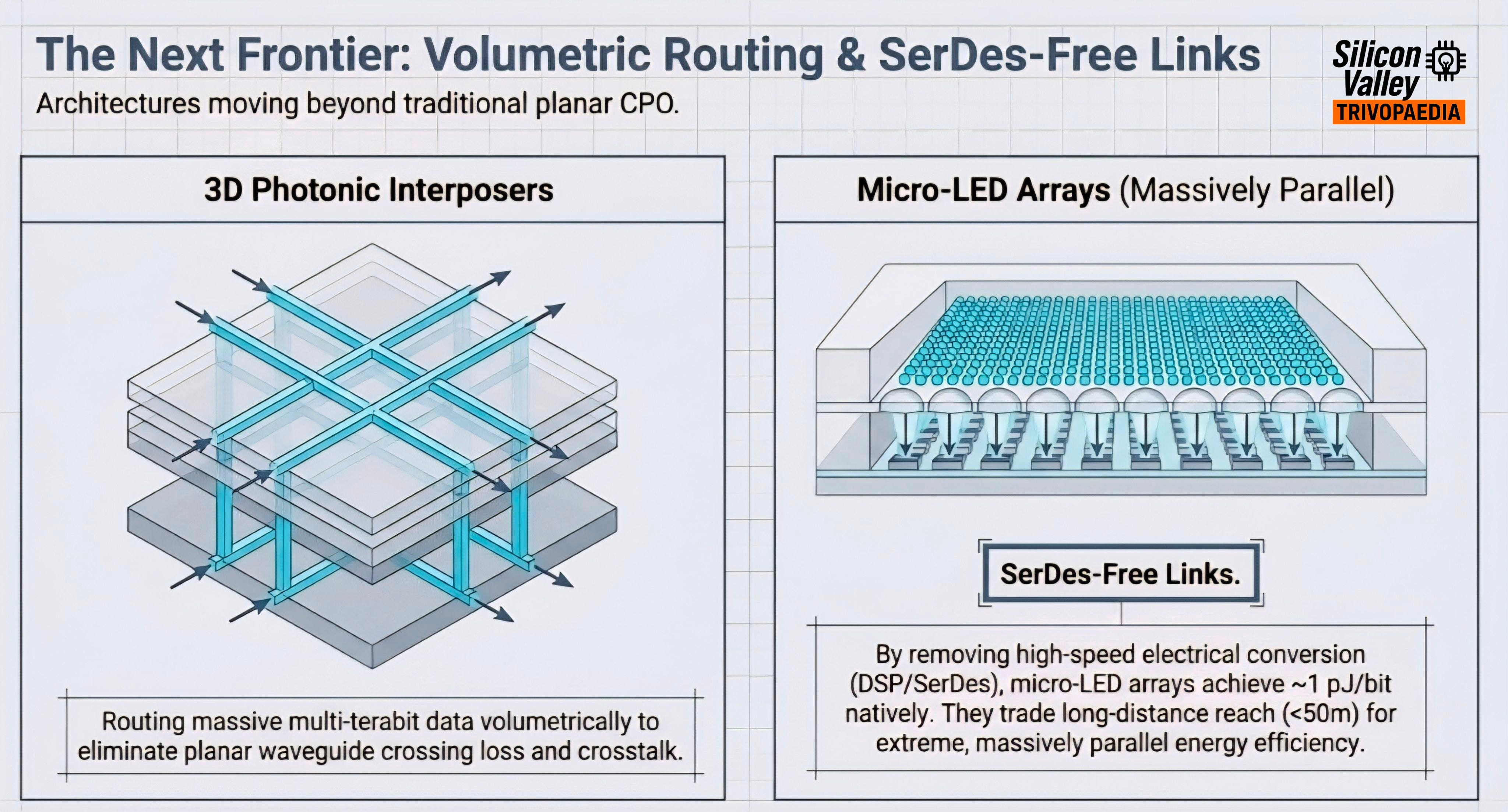
Lee points at ultrathin photonic materials and µLED parallelism as the next cut. Consistent with the review. Not a module you can order against HBM4E.
6. What SK added that the review would not say as a headline
The review will discuss optics-centric fabrics and memory pooling. It will not print “SK hynix’s technology roadmap” on the title. The newsroom will.
Hong does not talk like a DRAM datasheet owner. He talks like someone whose job is to put memory inside the customer’s system architecture. Lee is explicit about the prize: optical links at the memory interface lift the pin and capacity cage around the compute die, and let several accelerators share a pool.
HBM stays the fastest tier.
The architecture around HBM gets larger.
CPO is how a memory company stays in the room after the stack-height fight is over.
That is a coherent strategy sentence. It is not a commercial roadmap — no cadence, no socket, no power envelope for optical HBM I/O.
https://news.skhynix.com/en/cpo-in-nature-electronics/
7. What I am not taking from either text
I am not taking:
“Foundational standard by 2026” as an engineering fact.
<1 pJ/bit as something you can buy for a GPU package this year.
The newsroom pool diagram as a product.
What holds:
Training FLOPs and link bandwidth are on different slopes.
HBM closed one wall and revealed the next.
The remaining energy is in the electrical tax around the optical device.
Packaging integration, not a new III–V logo, is the near-term lever.
A memory company co-signing a CPO review is a systems bid, not a transceiver bid.
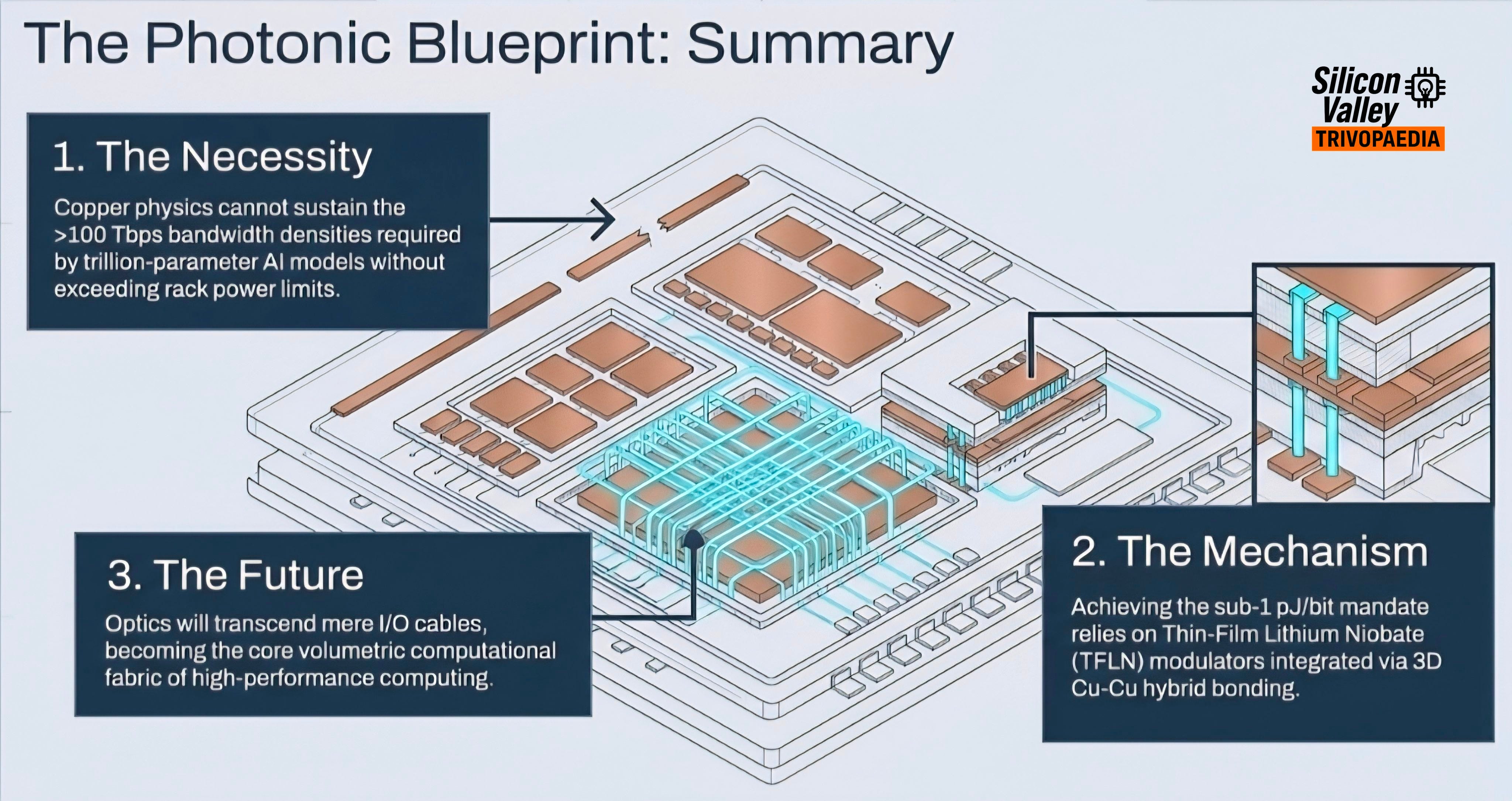
Copper cannot carry 100 Tbps-class node fabrics inside a 30–100 kW rack without eating the power budget. That is physics, not a vendor slide.
Optics in the package is the response that actually changes the energy and the reach. How far that optics is allowed to travel — to the switch, to the GPU, to the memory stack — is the argument SK chose to make in public. How soon anyone ships it at <1 pJ/bit, at yield, next to a hot compute die, is still a packaging problem.
The review mapped the domain. The newsroom told you which sentence a memory company wants attached to it. Neither one is a product. The product, when it exists, will be a bond pitch, a thermal loop, and a pJ number that survives the rack.
Sources
Byungsoo Kim et al., “Co-packaged optics for high-performance computing and artificial intelligence,” Nature Electronics 9, 853–867 (2026). https://doi.org/10.1038/s41928-026-01681-6
SK hynix Newsroom, 20 Aug 2026. https://news.skhynix.com/en/cpo-in-nature-electronics/
Reconstructed figures from @SVTrivo X:
 Papa Johns@SVTrivoThis weekend in Washington, DC, I finally sat down and read the full Nature Electronics review on co-packaged optics — not the abstract, the whole paper. Kim et al., Aug 2026. CPO for HPC and AI. HBM already fixed the package. Copper did not fix the rack. Thread. Charts below are…
 Papa Johns @SVTrivoCPO is becoming increasingly critical to break through the conventional data transmission bottlenecks of the AI era. https://t.co/qEzuSkcW77 https://t.co/L5uX0CKXKe5:45 AM · Aug 31, 2026 · 3.77K Views1 Reply · 1 Repost · 10 Likes