

Disclosure. I am long Cerebras (NASDAQ: CBRS). I am a working semiconductor designer, not a sell-side analyst. This is not a price target and not a recommendation. I was invited to Cerebras headquarters later this month for lunch and a data-center walkthrough. What follows is the brief I am carrying into that building.
A week after Hot Chips, the argument on X split into two questions that should never have been fused. Is the architecture garbage? And can this company be worth the multiple the tape is using?
The hallway version was cruder. Cerebras put Rubin in an adjacent column, talked about stitching wafers together, and put stacked DRAM on a roadmap slide. OpenAI showed Jalapeño. Nvidia showed a Groq-class LPX rack. The reconstruction that followed was tidy, and wrong in one direction, and right in another:
The wafer that was supposed to do everything now needs friends. Therefore the idea failed.
What ended is a pitch. The pitch was: one wafer, weights resident, no off-chip, no DRAM, no cluster politics. That sentence was already under stress when I read the S-1 in May. Hot Chips made the stress official.
What did not fail is the physical fact that still distinguishes the part. Almost a million small cores, each with its own SRAM, talking to neighbors in a single-cycle mesh on 46,225 mm² of silicon. That locality is real. It is also smaller than the models people now want to serve. The rest of this piece is about that gap — how Cerebras discovered it in public, and what it is building instead of pretending the gap is not there.
Three documents, three questions
I did not come to this company this week.
The first document is the S-1 I read while submitting an indication of interest on SoFi, because Robinhood did not have the deal. That filing answers a manufacturing question: how do you ship a chip the size of a dinner plate?
The second is Supernova, 18 August, Sean Lie on stage with CS-4. That event answers a product question: what do you sell when the dinner plate is no longer large enough?
The third is Hot Chips, late August, same machine, different room. That talk answers a peer question, and answers it badly in places: where does this sit next to Rubin, LPX, Jalapeño, and a memory industry that is stacking DRAM onto logic?
Read separately, each document sounds like a win. Read in order, they are a narrowing.
What the S-1 actually invented
The invention was never “the largest chip.” Large is the result. The inventions are the things that keep a wafer alive after the foundry has done what foundries do — print defects into 46,225 mm² of N5.
Scribe-line stitching. A normal 300 mm wafer is a 12×7 grid of reticles that will be sawed apart. Cerebras does not saw. An offset exposure of upper metal uses the scribe lanes as wires and ties the reticles into one mesh. No active devices live in that stitch. The stitch is only interconnect, which is why a defect there can be repaired with a spare link instead of killing the wafer.
Harvest, not purity. Each core is about 0.05 mm². On a conventional reticle-sized SoC, a particle in the wrong place scraps the die — or at least a large block — because the functions on that die are not interchangeable. The WSE is populated with about 970,000 identical cores and ships with about 900,000 enabled. The same particle retires a tile. The mesh routes around it. Cerebras quotes this as ~93% silicon utilization. That is not foundry die-sort yield. Friends who have worked yield will tell you the same thing. Utilization after harvest and a wafer-sort pass rate are different meters. Confusing them is how the sentence “their yields suck” gets written by people who are not wrong about margins and are wrong about topology.
A five-port mesh. Tile = core + local SRAM + router. Four cardinal ports and one port into the core. Lossless flow control, single-cycle neighbor hops. Die-to-die is a short, source-synchronous, high-metal bus with redundant lanes and a state machine that fails over. Across a wafer the stitch count is large enough that defects in the interface are assumed.
MemoryX and SwarmX. This is the part of the S-1 that aged. The cluster language in the filing is still a training language. MemoryX parks weights off-wafer and streams a layer at a time. SwarmX is a data-parallel fabric for broadcast and reduction, drawn up to 2,048 nodes. That architecture can train a model whose weights will never fit in 44 GB. It also throws away the only number that made the wafer special. On-wafer SRAM moves at 21 PB/s. Off-wafer I/O on a CS-3 is about 150 GB/s. Stream the model and the dinner plate becomes an expensive socket.
I wrote the first version of this in May, after the S-1, before the stock had a ticker that anyone could fight about:
Cerebras solved two fundamental constraints in semiconductors at the same time: die size limit + off-chip memory bottleneck. The WSE-3 turns an entire 300mm wafer into one monolithic chip, completely eliminates HBM, and packs 44GB of distributed on-chip SRAM… 21 PB/s.
— 12 May 2026


That paragraph is still the right description of one wafer doing what fits on one wafer. It is no longer a description of the product Cerebras is shipping into 2027.
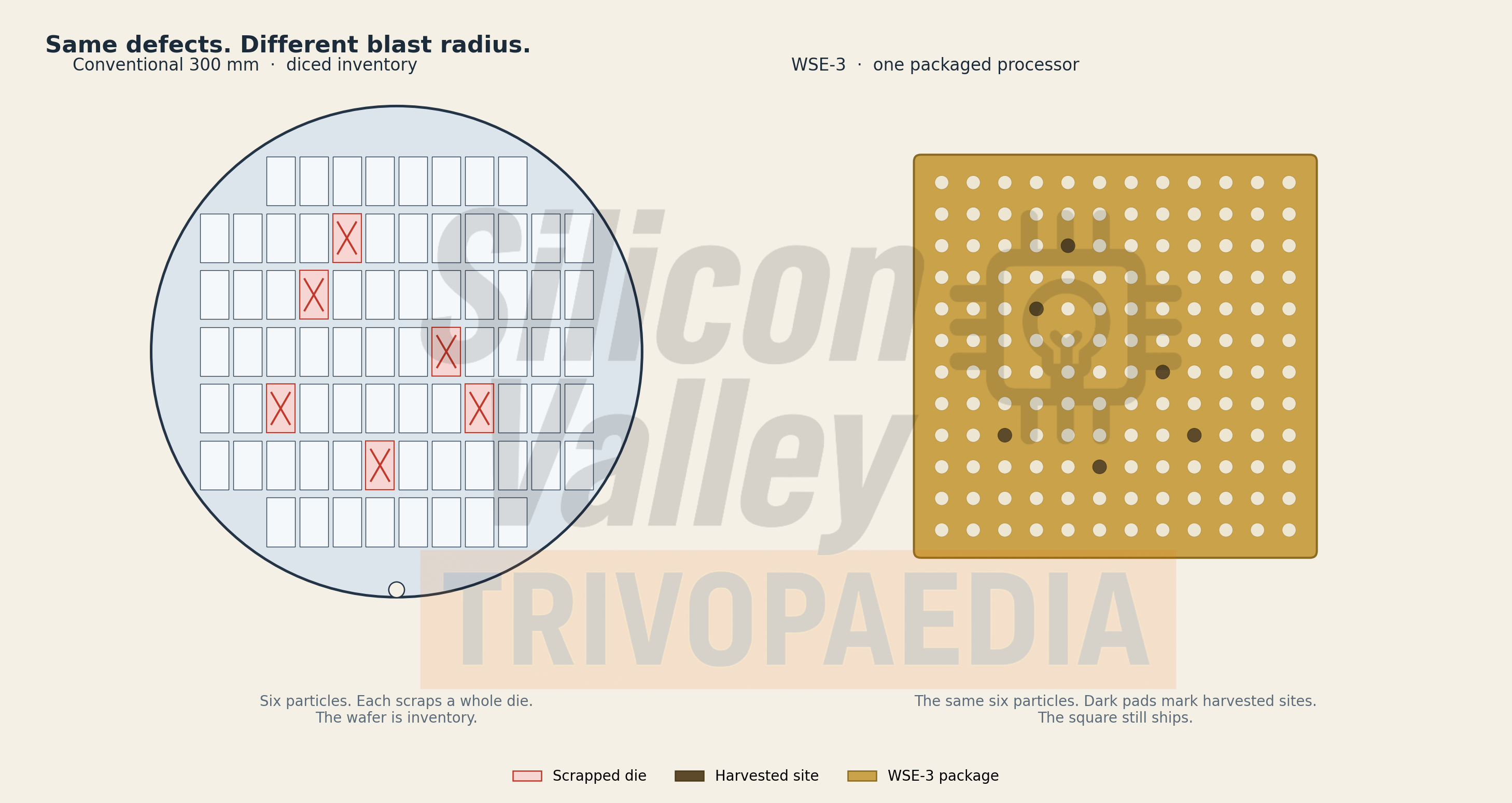
The first reaction was the correct engineering reaction
I have designed on nodes down to 2 nm. The first time someone described a 46,225 mm² processor to me, I said what every serious designer says.
Yield will be catastrophic. You cannot test it. You cannot route around that many defects.
Then the topology flips. Tiny identical cores. A reserve of about one percent. A mesh that treats a dead tile the way a datacenter treats a dead server. Weights that never leave SRAM if you keep the working set on the wafer. The sentence changes from insane to of course — not because the problems vanished, but because they were moved from process control to architecture.
I have had that conversation over dinner and on after-lunch walks more times than I can count. Ten minutes of the harvest story and the room changes register. That is why I was in the IPO. It is also why I added in the 401(k) after the IPO, the same way the Korean National Pension did. The technology was never the open question for me. The open question, which I wrote months ago and which the tape is still asking, was whether this thing earns money.
As a chip designer who has spent nearly three decades in Non-memory SoC, I still remember the exact second I first heard about Cerebras… “That’s insane. Yield will be catastrophic.” Then I studied the actual architecture… Suddenly the “insane” idea flipped into pure, shocking genius.
The technology was never the open question for me. The open question was always… “Earning money is the next problem with this amazing technology.”
— 17 August 2026

Hot Chips did not reopen the yield argument. It reopened the slogan.
From here the piece is for paid subscribers. Part 2 after the visit will live in the same post.
