

Originally published on X in May 2026. Updated and archived here as part of Silicon Valley Trivopaedia.
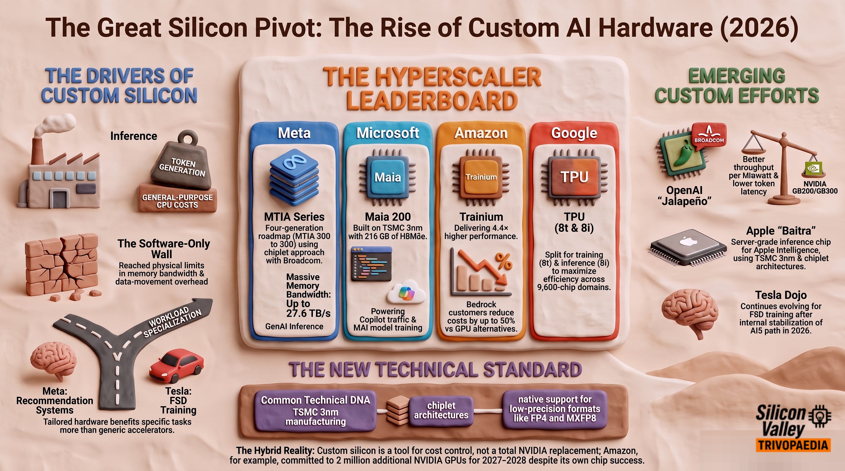
For years, leading AI companies focused primarily on software optimization. NVIDIA’s CUDA ecosystem, along with mature libraries like cuDNN, TensorRT, and NCCL, was so dominant that most organizations believed they could maintain a competitive edge through software alone. “Let NVIDIA handle the hardware; we’ll optimize on top of it” was the prevailing mindset.
That assumption began to break down around 2023–2024.
The explosion in model scale dramatically increased both training and inference costs. More importantly, inference — not training — became the dominant cost driver in real-world production systems. Software optimizations helped, but they eventually hit hard limits in memory bandwidth, data-movement overhead, and low-precision compute efficiency. These bottlenecks could no longer be fully solved at the software layer.
At the same time, NVIDIA’s supply constraints and premium pricing during the H100/H200 era created serious operational and financial pressure. Hyperscalers investing tens of billions of dollars in AI infrastructure started treating GPU cost and power consumption as core strategic risks, not just procurement issues.
Equally important was workload specialization. Meta’s recommendation systems, Google’s search and Gemini workloads, Amazon’s Bedrock services, and Tesla’s FSD training have very different computational characteristics than generic large language models. These workloads benefit from hardware tailored to specific patterns — massive KV-cache handling, sparse operations, aggressive low-precision formats — which general-purpose GPUs are not optimally designed for.
Advances in chiplet architecture, advanced packaging, and the maturity of TSMC’s 3nm process finally made it technically and economically viable for these companies to design their own silicon. The potential gains in power efficiency, silicon cost, and performance per dollar (often estimated at 30–50%+) became too significant to ignore.
As a result, several hyperscalers moved from “software on top of NVIDIA” to building custom ASICs purpose-built for their specific needs. Below is the state of the major efforts, originally written in mid-2026 and lightly updated after Hot Chips 2026.
1. Meta — MTIA Series: The Most Aggressive Multi-Generation Push
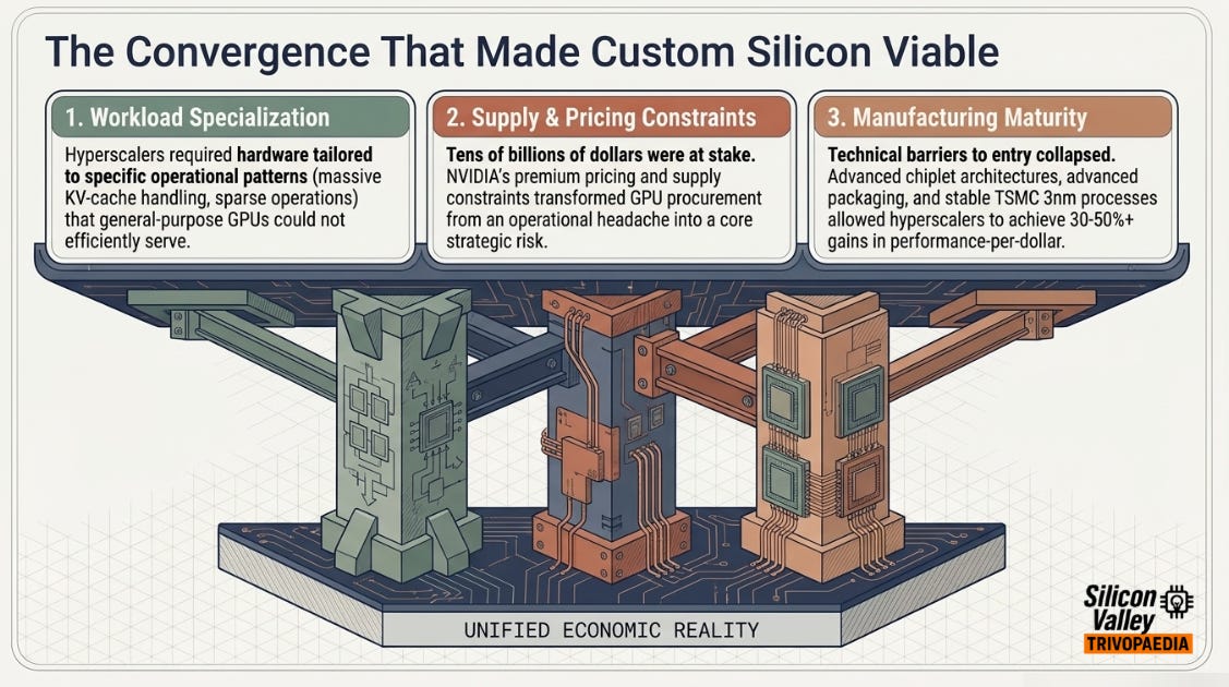
In March 2026, Meta announced four generations of its Meta Training and Inference Accelerator — MTIA 300, 400, 450, and 500 — developed with Broadcom on a chiplet-based approach.
MTIA 300 is in production, optimized for ranking and recommendation training.
MTIA 400 expands coverage to general GenAI workloads and supports large-scale 72-chip configurations. As of Hot Chips 2026 (late August), Meta presented MTIA 400 as the near-term workhorse, with rollout in 2026.
MTIA 450 and 500 are heavily optimized for GenAI inference. The standout improvement is memory bandwidth: MTIA 450 targets 18.4 TB/s, while MTIA 500 targets 27.6 TB/s with up to 512 GB of HBM. That directly helps large-context inference and high batch-size serving by keeping more KV cache in fast memory.
Meta’s ability to stack four generations in a short window reflects both the urgency of GenAI inference demand and the advantages of its chiplet + Broadcom partnership. The chips are already running at scale for Facebook and Instagram recommendations as well as Llama inference, with plans to expand further into training. Mass deployment of 450/500 is still slated for 2027.
2. Microsoft — Maia 200: Focused on Inference Economics
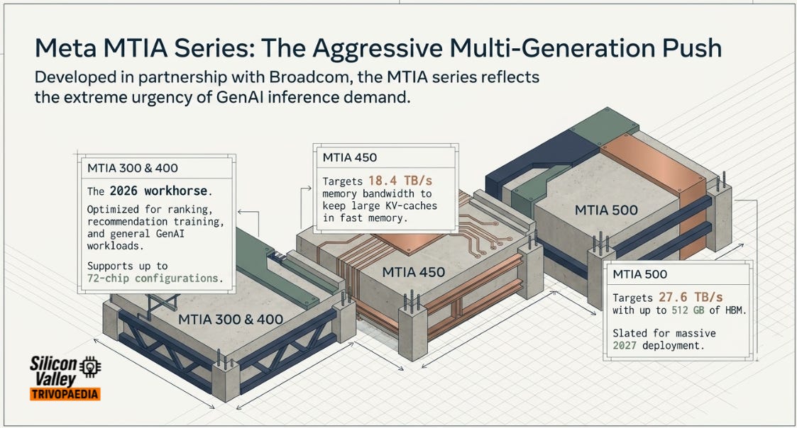
Announced in January 2026, Maia 200 is Microsoft’s clearest statement yet on custom silicon. It is purpose-built for inference, specifically the economics of token generation.
Built on TSMC 3nm with native FP8/FP4 tensor cores, it features 216 GB of HBM3e at 7 TB/s plus a large on-chip SRAM pool. Microsoft has claimed meaningful advantages versus competing custom chips from Amazon and Google on certain inference workloads.
By August 2026, the story had moved from announcement to architecture disclosure and production use:
Microsoft presented Maia 200 at Hot Chips 2026 (750W TDP class, ~10 PFLOPS FP4 in disclosed figures).
An arXiv paper described it as a software-defined dataflow system.
Microsoft’s own MAI models are being trained and served with co-design on Maia 200, and some Copilot traffic is already routing to first-party models running on this stack.
The chip is no longer a slide. It is inside Azure.
3. Amazon — Trainium3: The Most Production-Ready at Scale — and Still Buying NVIDIA
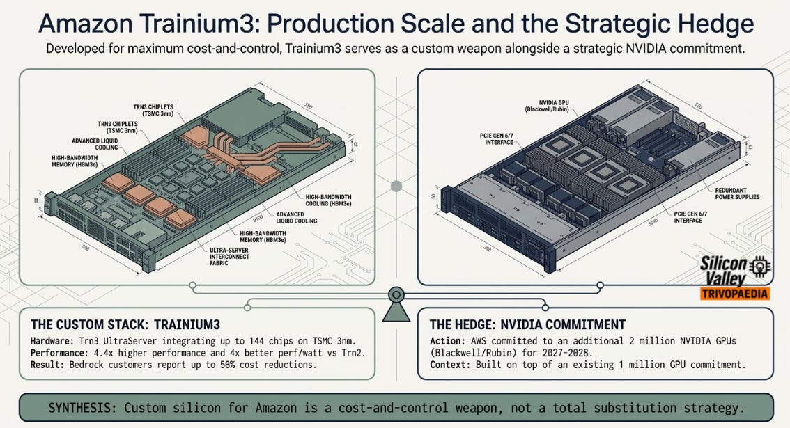
Trainium3, unveiled at re:Invent 2025 and now in broad production, remains one of the most mature custom AI chips in real-world use. Built on TSMC 3nm, it powers the Trn3 UltraServer, which can integrate up to 144 chips in a single system.
It delivers up to 4.4× higher performance and roughly 4× better performance per watt versus Trainium2, with strong support for MoE architectures and low-precision formats (MXFP8/MXFP4). Multiple Bedrock customers have reported cost reductions of up to 50% versus GPU-based alternatives. Amazon’s advantage is not just the die — it is the tightly integrated server + software system.
The August 2026 update matters: Amazon is not walking away from NVIDIA. AWS committed to another 2 million NVIDIA GPUs for 2027–2028 (Blackwell Ultra / Rubin / Rubin Ultra), on top of an earlier ~1 million commitment. Custom silicon is a cost-and-control weapon. It is not a full substitution strategy — at least not yet.
4. Google — Ironwood, Then TPU v8
Google’s seventh-generation TPU, Ironwood, was designed for the “age of inference” while keeping strong training capability. It claimed up to 10× peak performance over TPU v5p and more than 4× per-chip improvement versus Trillium (v6e). Its distinctive strength is extreme scale: Superpods connecting thousands of chips, backed by Pathways.
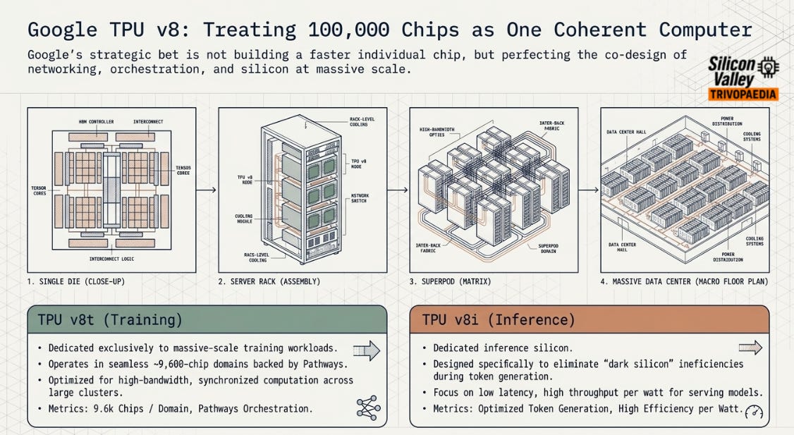
By spring/summer 2026, Google had already moved to an eighth-generation split:
TPU 8t for training
TPU 8i for inference
Hot Chips 2026 made the systems-level ambition explicit: a ~9,600-chip training domain, dedicated inference silicon to avoid dark silicon, and continued co-design of networking + orchestration. Google’s bet is not “a faster chip.” It is treating tens or hundreds of thousands of chips as one coherent computer.
Ironwood is the previous chapter. TPU v8 is the current one.
5. Other Notable Efforts
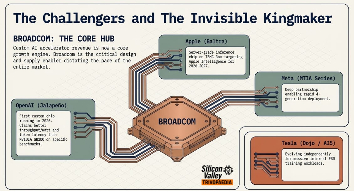
Tesla Dojo. Continues to evolve for FSD training and large-scale internal AI workloads. Development on later Dojo generations resumed in 2026 after Tesla stabilized its AI5 path.
Apple Baltra. Working with Broadcom on a server-grade inference chip (2026–2027 window), chiplet design on TSMC 3nm, aimed at Apple Intelligence workloads.
OpenAI. The first custom chip, previously discussed as Project Titan, surfaced publicly as Jalapeño (with Broadcom). Engineering samples were running in 2026; Hot Chips 2026 and OpenAI’s own disclosures claimed better throughput per kilowatt and lower token latency than NVIDIA GB200/GB300-class systems on selected public inference benchmarks. Initial deployment is targeted for later 2026, with next generations already in design. This is the most important update since the original May post.
Broadcom. Still the critical enabler — design and supply partner for Meta, OpenAI, and others. Custom AI accelerator revenue has become a core growth engine, not a side business.
6. Key Takeaways
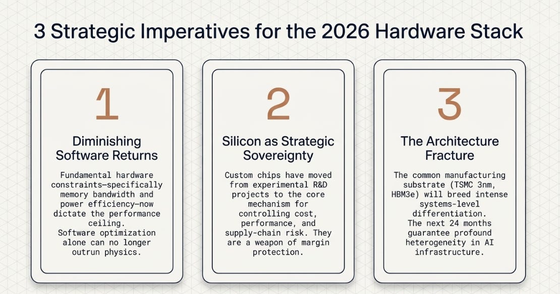
The shift toward custom ASICs is not merely about raw performance. It reflects a recognition that software optimization alone has hit diminishing returns against fundamental hardware constraints—especially memory bandwidth, power efficiency, and workload-specific compute patterns.
Common technical themes:
Chiplet architectures
Aggressive HBM (HBM3e now, HBM4 incoming)
Native low-precision formats (FP8, FP4, MXFP)
TSMC 3nm as the common manufacturing substrate
Differentiation at architecture and systems level (rack, fabric, compiler, serving stack)
For NVIDIA, this is a long-term structural challenge even while CUDA, CUDA-X, and broad applicability remain powerful moats. Amazon’s latest GPU order is the clearest proof that NVIDIA is not being replaced overnight. It is being complemented and selectively displaced where workloads are stable enough to justify a custom die.
For hyperscalers, custom silicon has moved from an interesting side project to a core strategic capability: control over cost, performance, power, and supply-chain risk.
The next 18–24 months will likely bring even more aggressive roadmaps and greater heterogeneity in AI infrastructure. Each major player is doubling down on hardware tailored to its own strengths. The industry is no longer one GPU architecture with many software stacks. It is becoming many architectures with competing full stacks.
References
Meta. (March 11, 2026). Expanding Meta’s Custom Silicon to Power Our AI Workloads.
ServeTheHome. (August 25, 2026). Meta’s MTIA Custom AI Silicon at Hot Chips 2026.
Microsoft. (January 26, 2026). Maia 200: The AI accelerator built for inference.
ServeTheHome. (August 25, 2026). Microsoft’s Maia 200 AI Accelerator at Hot Chips 2026.
Hoefler et al. (August 2026). Maia 200: A Software Defined Dataflow System for Large-scale AI Acceleration. arXiv:2608.24664.
AWS. (December 2025). Amazon EC2 Trn3 UltraServers. re:Invent 2025.
TechCrunch / NVIDIA earnings week. (August 26, 2026). Amazon’s expanded NVIDIA GPU commitment.
Google Cloud. Ironwood TPU materials (2025–2026) and TPU 8t / 8i technical deep dive (April 2026).
ServeTheHome. (August 25, 2026). Google’s TPUv8s for Training and Inference at Hot Chips 2026.
OpenAI. (June 24, 2026). OpenAI and Broadcom unveil LLM-optimized inference chip.
OpenAI. (August 24–25, 2026). Jalapeño performance disclosures / Hot Chips coverage.
Reuters / HPCwire. (March 11, 2026). Meta in-house AI chip coverage.